Wednesday, December 18, 2013
Browse »
home»
a
»
build
»
charge
»
circuit
»
diagram
»
pump
»
regulated
»
Build a Regulated Charge Pump Circuit Diagram

Build a Regulated Charge Pump Circuit Diagram
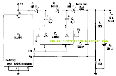
How to Build a Regulated Charge Pump Circuit Diagram. The dc-dc converter substitutes a voltage triplet in place of the external inductor and the diode that`s typically associated with the switching regulator, IC1. Inverting and non inverting amplifiers in the MOS-FET-driver (IC2) activate a diode-capacitor tripling network (D1 through D3, CI through C3).
A 50-kHz oscillator residing within IC1 produces the EXT signal (pin 6), IC2 converts this signal into drive signals (180° out of phase) for the tripler. The resulting charge-discharge action in the capacitors recharges C3 toward 10 V every 20 The ferrite bead limits output ripple to about 20-mVpp for a 50-mA load. Conversion efficiency is about 70% for the 5-V input, 10-V output configuration.
Regulated Charge Pump Circuit Diagram

Subscribe to:
Post Comments (Atom)
No comments:
Post a Comment
Note: Only a member of this blog may post a comment.