Friday, December 27, 2013
Simple linear Regulator Circuit Diagram

Thursday, December 26, 2013
LDR Based 12V White LED Driver for up to 30 LEDs
 |
| 30 White LEDs Driver Circuit Diagram |
Instead of around 1.8V to 2V or thereabouts, they normally require more than 3V to produce their rated brightness. In fact, if you are driving a bunch of them you need to drive them all at constant current otherwise their individual brightness tends to vary markedly. However, if you only have a 12V supply available, you can only put two or maybe three LEDs in series together with a constant current source and this leads to poor efficiency.

The approach in this circuit is to boost the 12V supply to something around 21V and this means that we can have groups of five LEDs, each in series with their own current source transistors. The result is a single PC board with the drive circuitry and 30 white LEDs. It can be used for lighting in caravans and recreational vehicles, emergency lighting or whatever application you can think of. Current drain is around 190mA at 12V.
Circuit description
Now let’s have a look at the circuit of Fig.1. It uses just one IC (a 4093 quad NAND Schmitt trigger gate package), a few transistors and diodes, 30 white LEDs and not much else. So where is the familiar boost converter circuit? Answer: there isn’t one or least not one with an inductor switched by a Mosfet. Instead, there is a charge pump inverter, comprising IC1c, transistors Q2 & Q3, Schottky diodes D1 & D2 and a few capacitors. It works as follows:

IC1c is connected as an inverter oscillator and its running frequency of about 30kHz is determined mainly by the 6.8kΩ resistor between pins 8 & 10 together with the 4.7nF capacitor at pin 8. This produces a rectangular waveform (not quite square but pretty close) at pin 10 to drive complementary switching transistors Q2 & Q3.
The waveform at their commoned emitters drives a diode pump consisting of two 100μF capacitors and Schottky diodes D1 & D2. The waveform generated by the circuit can be seen in the scope photo of Fig.2.
RS flipflop
Oscillator IC1c is controlled by an RS (Reset/Set) flipflop comprising the two NAND gates IC1a & IC1b and this is controlled by pushbutton switches S1 and S2. Normally, this has its pin 4 low and pins 1 & 6 are pulled high via 470kΩ resistors. Momentarily closing S1 (ON) pulls pin 6 low, causing the flipflop to change state so that pin 4 now goes high to enable IC1c which now oscillates at 30kHz.

The 30kHz waveform produced by transistors Q2 & Q3 drives the diode pump referred to earlier and this develops about 21V to drive the LED columns. Each column of five white LEDs is driven by its own current source transistor which has a 33Ω emitter resistor. The bases of all six current source transistors (Q4-Q9) are driven from pin 4 of IC1b via a 6.8kΩ resistor and clamped to a maximum of +1.2V by diodes D3 & D4.
Subtract the 0.6V between the base and emitter of each transistor and you are left with 0.6V across each 33Ω resistor, thus setting the LED drive current to 18mA. Switching the circuit off is accomplished by pushing the OFF switch, S2. This momentarily pulls pin 1 low to toggle the RS flipflop, thus causing pin 4 to go low. This disables IC1c, Q2 & Q3 and also turns off the current source transistors.
Note that there is an interesting wrinkle to this drive circuit, because there is no On/Off switch. This means that the current source transistors must be turned off otherwise they would continue to draw current from the 12V supply even when the circuit is nominally off. The current path may not be obvious but it is via the boost circuit’s diodes, D1 & D2.
Auto on/off
As well as using the pushbutton switches S1 & S2 to turn the circuit on and off, there is also a facility to automatically turn the circuit on and off depending on ambient light levels. Links L1 & L2 can be used to provide Auto On and Auto Off respectively and these features can be used separately or together.

An LDR (light dependent resistor) is used to monitor the ambient light level. When light falls upon it, it pulls the base of Q1 low, causing pins 12 & 11 of IC1d to go low and its pin 11 to go high. When darkness falls (or the room lights go out), the process is reversed. Depending on whether you have one or both links connected, you can use the pushbuttons to turn the circuit on and off and have it turn on and/off automatically as well.
Q1 also drives a red high brightness LED (LED1) at very low current, via a 470kΩ resistor. This is a bit of a gimmick but it does have the benefit of showing that this part of the circuit is working, if you have to trouble-shoot it.
Note:
Pins 1 & 2, 5 & 6 and 8 & 9 of IC1 on the circuit are all swapped. The PC board overlay diagram is correct.
Simple Multivoltage Power Supply Circuit Diagram
Multivoltage Power Supply Circuit Diagram

Wednesday, December 25, 2013
Two Wire Temperature Sensor
Remote temperature measurements have to be linked by some sort of cable to the relevant test instrument. Normally, this is a three-core cable: one core for the signal and the other two for the supply lines. If the link is required to be a two-core cable, one of the supply lines and the signal line have to be combined. This is possible with, for instance, temperature sensors LM334 and LM335. However, these devices provide an output that is directly proportional to absolute temperature and this is not always a practical proposition.
Circuit diagram :

Two-Wire Temperature Sensor Circuit Diagram
If an output signal that is directly proportional to the celsius temperature scale is desired, the present circuit, which uses a Type LM45 sensor, offers a good solution. The LM45 sensor is powered by an alternating voltage, while its out-put is a direct voltage.
The supply to the sensor is provided by a sine-wave generator, based on A 1 and A 2 (see diagram). The alternating volt-age is applied to the signal line in the two-core cable via coupling capacitor C 6 .
The sensor contains a volt-age-doubling rectifier formed by D 1 -D 2 -C 1 -C 2 . This network converts the applied alternating voltage into a direct voltage. Resistor R 2 isolates the output from the load capacitance, while choke L 1 couples the output signal of the sensor to the signal line in the cable. Choke L 1 and capacitor C 2 protect the output against the alternating voltage present on the line.
At the other end of the link, network R 3 -L 2 -C 4 forms a low-pass section that prevents the alternating supply voltage from combining with the sensor out-put. Capacitor C 5 prevents a direct current through R 3 , since this would attenuate the temper-ature-dependent voltage.
The output load should have a high resistance, some 100 kΩ or even higher. The circuit draws a current of a few mA.
Simple UPS Power Supply
This circuit is a simple form of the commercial UPS, the circuit provides a constant regulated 5 Volt output and an unregulated 12 Volt supply. In the event of electrical supply line failure the battery takes over, with no spikes on the regulated supply.

Notes:
This circuit can be adapted for other regulated and unregulated voltages by using different regulators and batteries. For a 15 Volt regulated supply use two 12 Volt batteries in series and a 7815 regulator. There is a lot of flexibility in this circuit.
TR1 has a primary matched to the local electrical supply which is 240 Volts in the UK. The secondary winding should be rated at least 12 Volts at 2 amp, but can be higher, for example 15 Volts. FS1 is a slow blow type and protects against short circuits on the output, or indeed a faulty cell in a rechargeable battery. LED 1 will light ONLY when the electricity supply is present, with a power failure the LED will go out and output voltage is maintained by the battery. The circuit below simulates a working circuit with mains power applied:

Note that in all cases the 5 Volt regulated supply is maintained constantly, whilst the unregulated supply will vary a few volts.

Standby Capacity
The ability to maintain the regulated supply with no electrical supply depends on the load taken from the UPS and also the Ampere hour capacity of the battery. If you were using a 7A/h 12 Volt battery and load from the 5 Volt regulator was 0.5 Amp (and no load from the unregulated supply) then the regulated supply would be maintained for around 14 hours. Greater A/h capacity batteries would provide a longer standby time, and vice versa.
Tuesday, December 24, 2013
Variable Zener Diode Circuit Diagram

Simple Battery Temperature Sensing Nicad Charger

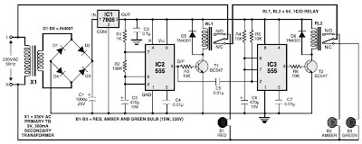
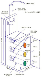
Traffic Light Controller
Monday, December 23, 2013
Optical technology is tiny particles can be captured
The most common problem is reported use of micro-cellular phone may display you have five full signal strength. Call directly into voicemail ring. The reason is because the micro cellular behind the idea under the premise of the construction site, to build a miniature battery. The microcell tether recent site, and then take advantage of the Wi-Fi signal, in order to strengthen their reception and transmission bandwidth.
The pursuit of low-cost mobile phone maker has also spawned a number of new business opportunities. The original baseband IC field is Texas Instruments. However, these always attaches great importance to the base price of the domestic mobile phone manufacturers in the industry with handset manufacturers dissatisfaction, a significant loss. Once a suitable alternative suppliers, domestic mobile phone manufacturers immediately anti-Ge. Other suppliers is Taiwans largest IC design company MediaTek. MediaTek low-cost baseband IC quickly captured the mainland market, almost all of the Chinese mobile phone manufacturers, including Asus and BenQ MediaTek customers. After the installation is complete, turn off the circuit breaker or phone boosters, and turn on the power switch. Texas Instruments beat beaten. MediaTek are cashing overflow, MediaTeks report shows, pre-tax income of the U.S. dollar, the Taiwan stock market profits. Most of the mobile phone industry chain manufacturers and performance of domestic mobile phone manufacturers.
Keeping that in mind, rarely introduced new equipment call phone signal booster, market a few years ago. , Phone booster introduced several years ago, but as time goes by, and its technology has been updated. In such a small period of time to introduce mobile phone supercharger technology has improvised a lot of times, this is a cell phone signal amplifier on the market a wide range of reasons.
Low cost Step down Converter with Wide Input Voltage Range
The circuit described here is mostly aimed at development engineers who are looking for an economical step-down converter which offers a wide input volt- age range. As a rule this type of circuit employs a step-down converter with integrated switching element. However, by using a more discrete solution it is possible to reduce the total cost of the step- down converter, especially when manufacturing in quantity. The TL5001A is a low-cost PWM controller which is ideal for this project.

The input voltage range for the step-down converter described here is from 8 V to 30 V, with an output voltage of 5 V and a maximum output current of 1.5 A.
When the input voltage is applied the PWM output of IC1 is enabled, taking one end of the voltage divider formed by R1 and R2 to ground potential. The cur-rent through the voltage divider will then be at most 25 mA: this value is obtained by dividing the maximum input voltage (30 V) minus the saturation voltage of the output driver (2 V) by the total resistance of the voltage divider (1.1 kΩ ). T1 and T3 together form an NPN/PNP driver stage to charge the gate capacitance of P-channel MOSFET T2 as quickly as possible, and then, at the turn-off point, discharge it again.
The base-emitter junction of T3 goes into a conducting state when the PWM output is active and a voltage is dropped across R2. T3 will then also conduct from collector to emitter and the gate capacitance of T2 will be discharged down to about 800 mV. The P-channel MOSFET will then conduct from drain to source. If the open-collector output of the controller is deactivated, a negligibly small current flows through resistor R2 and the base of T1 will be raised to the input voltage level. The base-emitter junction of T1 will then conduct and the gate capacitance of T2 will be charged up to the input voltage level through the collector and emitter of T1. The P-channel MOSFET will then no longer conduct from drain to source. This driver circuit constructed from discrete components is very fast, giving very quick switch-over times.
Diodes D2 and D3 provide voltage limiting for the P-channel MOSFET, whose maximum gate-source voltage is 20 V. If the Zener voltage of diode D2 is exceeded it starts to conduct; when the forward voltage of diode D3 is also exceeded, the two diodes together clamp the gate-source voltage to approximately 19 V.
The switching frequency is set at approximately 100 kHz, which gives a good compromise between efficiency and component size.
Finally, a few notes on component selection. All resistors are 1/16 W, 1 %. Apart from electrolytic C1 all the capacitors are ceramic types. For the two larger values (C2 and C5) the following are used:
C2 is a Murata type GRM21BR71C105KA01 ceramic capacitor, 1 µF, 16 V, X7R, 10 %;
C5 is a Murata type GRM32ER60J476ME20 ceramic capacitor, 47 µF, 6.3 V, X5R, 10 %.
D1 (Fairchild type MBRS340T3) is a 40 V/3 A Schottky diode. Coil L1 is a Würth WE-PD power choke type 744771147, 47 µH, 2.21 A, 75 mΩ.
T1 (BC846) and T3 (BC856) are 60 V, 200 mA, 310 mW complementary bipolar transistors from Vishay.
The TL5001AID (IC1) is a low-cost PWM controller with an open-collector output from Texas Instruments.
Author : Dirk Gehrke Copyright : Elektor
Sunday, December 22, 2013
Preregulator for Power Supply Circuit Diagram
Preregulator for Power Supply Circuit Diagram

The voltage Vc decreases until Vc = V0 = V at which point the Darlington pair fires the SCR, charging the filter capacitor to a higher voltage VC1 in less than half the period of the input voltage. The component values, shown are for a 0 - 250-V, 3-A power supply.
Build a Efficient Negative Voltage Regulator Circuit Diagram

Power Supply Balance Indicator Circuit Diagram

Saturday, December 21, 2013
Simple Equipment on reminder Circuit Diagram
Equipment on reminder Circuit Diagram

Datasheet of 24C32
Datasheet file: Click here to download 24C32.pdf datasheet.
Friday, December 20, 2013
Simple Efficient Supply Splitter Circuit Diagram

40 LED Bicycle Light

A single LED is placed in series with the base of the PNP transistor so that the lower 20 LEDs turn off when the 555 output goes high during the T1 time interval. The high output level of the 555 timer is 1.7 volts less than the supply voltage. Adding the LED increases the forward voltage required for the PNP transistor to about 2.7 volts so that the 1.7 volt difference from supply to the output is insufficient to turn on the transistor.
Each LED is supplied with about 20mA of current for a total of 220mA. The circuit should work with additional LEDs up to about 40 for each group, or 81 total. The circuit will also work with fewer LEDs so it could be assembled and tested with just 5 LEDs (two groups of two plus one) before adding the others.
Thursday, December 19, 2013
Telephone Ringer
Telephone Ringer Circuit Diagram

The expert group is making every effort to enhance the design of the Cell Phone Jammers system
The standard test signal I1: is GsM modulated carrier signal, and its structure in accordance with the GSM signal burst (burst, as burst or short burst. Below) structure, but its all modulation bits (including the burst of part of the training sequence) are directly random or pseudo-random data stream. (5) The standard test signal I2: a standard GSM modulation signal, but with the C1 signal is different from the unexpected part of the training sequence of the standard GSM training sequence, but the burst of data bits (including bits 58 and 59) are random or pseudo-random data stream. Using the same standard RF cable and adapters, including adapters, including the requirements of the GSM bands between the channel loss is less than 0.5dB, loss of value of the difference is less than 0.2dB; DCS frequency band between the loss of each channel is less than 1dB, loss value difference is less than 0.3dB, with characteristic impedance adapter should be within 50 ± 5 ohms. The table will contain the result of quantity computation of Cell Phone Jammers .I use the above principles and interface technology to develop a project: Highway display guidance system. Installed on the highway in front of the LED display shows real-time road vehicle traffic situation and weather and climate conditions, advise and guide the driver, the correct driver. The use of the system to some extent, eliminate a lot of traffic hazards, thereby safeguarding the smooth flow of road safety and peoples lives and property. The system consists of the control center and several display screen. Control center in real time the latest information sent to the display. Building control center communication link with the display terminal, the traditional method of laying fiber optic cable with the cable or the realization, or build a private wireless network allowing wireless. Because of the special nature of the highway, the control center and the distance between the display terminal is usually very far, two programs must invest a lot of money and huge construction effort.
Typically, short message service SMS-based wireless data transmission monitoring and control system for a point to multipoint wireless two-way data communication and remote control system, shown in Figure 1. System control center or command center for data, from computer networks, databases, electronic map and GSM communication interface. The main control center complete the information and data transceiver and finishing: on the one hand, to receive various control points to upload information and data, and put them in the appropriate database and distributed to the appropriate monitoring computer in order to achieve the various monitoring points monitoring and management; another aspect, a computer control center monitors the response issued by the various monitoring points of the control information, and to the information issued to the corresponding control points to achieve the point of monitoring equipment for control purposes.
Mini Ups System
Mini Ups System Circuit diagram:

Wednesday, December 18, 2013
Build a Regulated Charge Pump Circuit Diagram

Simple 12 Volt 30 Amp PSU Circuit Diagram

The input transformer is likely to be the most expensive part of the entire project. As an alternative, a couple of 12 Volt car batteries could be used. The input voltage to the regulator must be at least several volts higher than the output voltage (12V) so that the regulator can maintain its output. If a transformer is used, then the rectifier diodes must be capable of passing a very high peak forward current, typically 100amps or more. The 7812 IC will only pass 1 amp or less of the output current, the remainder being supplied by the outboard pass transistors. As the circuit is designed to handle loads of up to 30 amps, then six TIP2955 are wired in parallel to meet this demand.

This circuit is a fine example of Kirchoffs current and voltage laws. To summarise, the sum of the currents entering a junction, must equal the current leaving the junction, and the voltages around a loop must equal zero. For example, in the diagram above, the input voltage is 24 volts. 4 volts is dropped across R7 and 20 volts across the regulator input, 24 -4 -20 =0. At the output :- the total load current is 30 amps, the regulator supplies 0.866 A and the 6 transistors 4.855 Amp each , 30 = 6 * 4.855 + 0.866. Each power transistor contributes around 4.86 A to the load. The base current is about 138 mA per transistor. A DC current gain of 35 at a collector current of 6 amp is required.
Tuesday, December 17, 2013
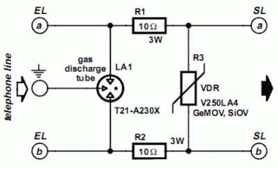
Protection For Telephone Line Circuit
Protection Circuit Diagram For Telephone Line :
Build Motorcycle Alarm Circuit Diagram

cell phone jammer will not intercept on the base station
Visible, smart phones, large screen, large screen products favored by the users. Chinese mobile phone market in June 2011, the smart phone market with different screen sizes attention to the proportion of contrast. Case Study: Apples share of continued expansion. Apples global handset market share continued to expand. According to the U.S. market research firm Gartner statistics show that, since 2007, Apple introduced the iPhone smart phone, smart phone market, the pattern began to change. In 2008, Apple alone an iPhone, the global market share has reached 8.2 percent, while the first quarter of 2011, only three years, alone, four generations of iPhone products, Apples market share has reached 16.8%, to become the worlds first The three operating systems. cell phone jammer will just influence the downlink.
2007-2011Q1 Apple Worldwide sales of mobile phones and smart phone market share trend. Data sources Gartner, data management: ZDC. Apple user attention in the smart phone market in China is climbing. Rattling trend in the global mobile phone market with Apple, the Apple in the smartphone market, but also showed the fierce attacks, especially in cooperation with China Unicom, Apple users attention from record highs. The ZDC monitoring data show that the smart phone market in China in June 2011, Apple accounted for 9.2 percent of the concern proportion, only a difference of 2.6 percent and Motorola. In addition, from Apple released the data, the establishment of the ecosystem and no brand. This is a considerate design for cell phone jammer .
Since 2011, the three operators for 3G mobile terminals, a number of Central Purchasing universal low-priced products has always been an important source of new 3G subscribers, new subscribers expected to reach the end of universal terminal undoubtedly become the focus of the tender object, and an important platform to promote value-added services as operators necessary to support the role of popular intelligent terminal to enhance 3G users overall ARPU value are bound to become the top priority of purchases and sales. Sino Market monitoring data show that in October this year, 3G smart market 700 to 1500 the proportion of the price reached 54.7%, 24.6% increase compared to same period last year, up significantly. The insulation feature of cell phone jammer is very important for the customer.Products, the number of 3G thousands of intelligent machines models increase from 15 in October 2010 to October 2011, 123 models, thousands of intelligent machines has become a new force of the smart phone market. The low-end market into focus. IPhone users and thousands of intelligent machines the user using the data flow to compare, you can find iPhone users monthly data traffic is not significantly higher.